PCB Prototype the Easy Way
Full feature custom PCB prototype service.
9:00 - 18:00, Mon.- Fri. (GMT+8)
9:00 - 12:00, Sat. (GMT+8)
(Except Chinese public holidays)
PCB Prototype the Easy Way
Full feature custom PCB prototype service.
9:00 - 18:00, Mon.- Fri. (GMT+8)
9:00 - 12:00, Sat. (GMT+8)
(Except Chinese public holidays)
PCB milling is a machining process that involves controlling the depth to remove specific portions of the circuit board material in order to recreate signal paths, solder pads and structures according to patterns from a digtal circuit board plan known as a layout file.
Furthermore, PCB milling is a subtractive process similar to commonly used chemical etching techniques. However, PCB milling does not involve any chemical substances, making it suitable for use in general home or office environments without the need for handling hazardous chemicals. Due to the use of milling equipment for electrical isolation, PCB milling is safer than chemical etching.
Minimum mill tool diameter is 0.8mm,standard mill tool diameter is 2.0mm,special mill tool diameter is 0.8mm≤Ø≤2.0mm.As described in the table below.
| Design Parameter | Value |
| Minimum mill tool diameter | 0.8mm |
| Standard mill tool diameter | 2.0mm |
| Special mill tool diameter | 0.8mm≤Ø≤2.0mm |
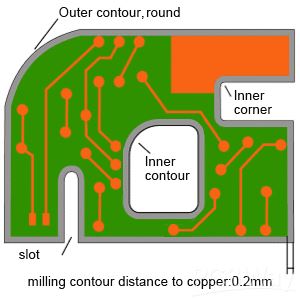
The inner and outer contours of the board can be processed according to customer requirements. The outer corners of the contour can be made as 90° angles or rounded corners as per the customer's request. However, the inner corners of the contour must have a minimum radius equal to the milling cutter radius.

The contours and inner openings of PCBs are usually milled, following the following rules:
In general, milling does not require any additional charges.
Please refrain from milling the copper to ensure the durability of the circuit board and reduce the risk of injury.
To prevent issues with measurements and dimensions, a line width of 0.2mm should be used to indicate the inner and outer contours of the PCB. Typically, the traces are routed at the center of the lines.
PCB milling offers advantages for prototype production and certain specialized PCB designs, with the biggest benefit being the absence of chemicals involved in PCB fabrication.
Milling cutters can be changed according to requirements.
Using CNC machines can help speed up the process of prototype production. If you already use CNC machines for drilling, they can handle both milling and cutting simultaneously, as CNC machines are highly useful for drilling, milling, and cutting operations.
In some cases, PCBs produced through milling are difficult to achieve with wet etching and require subsequent manual drilling, both of which incur higher costs compared to conventional milling.
Cut-out
Milling slots
Pocket milling
V-scoring
Separating panels
Cutting heat sink cavities
More information check here: